PECVD solves this by substituting plasma energy for thermal energy, enabling high-quality thin film deposition at temperatures as low as room temperature to 350°C. For advanced packaging applications, demonstrated process temperatures go as low as 100–110°C.
This guide covers how PECVD works mechanically, where it outperforms conventional CVD and PVD, its primary industrial applications, and how to select the right deposition technology for a given application — written for engineers and technical decision-makers evaluating coating process options.
Key Takeaways
- PECVD deposits thin films at room temperature to 350°C, vs. 600–800°C for conventional CVD
- Plasma energy drives chemical reactions, enabling low thermal budgets without sacrificing film quality
- Films are highly conformal, coating trenches, sidewalls, and complex geometries that PVD cannot reach
- Process parameters (RF power, gas ratios, pressure) directly control hardness, refractive index, and film stress
- Deposited materials include SiO₂, Si₃N₄, amorphous silicon, and Diamond-like Carbon (DLC)
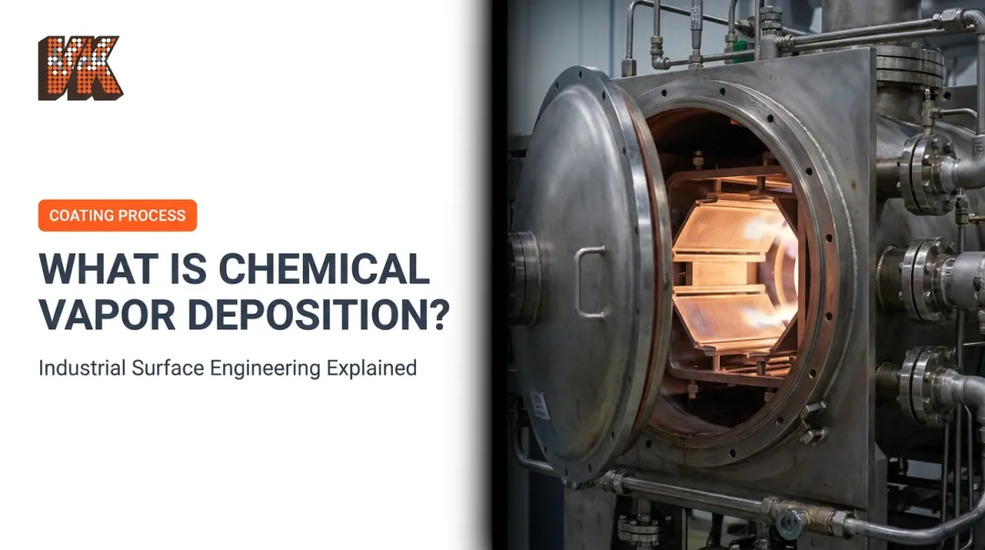
How Does PECVD Work?
Chamber Setup and Gas Delivery
The substrate sits inside a vacuum deposition chamber between two electrodes. Precursor gases — for example, silane (SiH₄) with ammonia (NH₃) for silicon nitride deposition — are introduced alongside inert carrier gases such as argon or nitrogen. A showerhead fixture distributes gases evenly across the substrate surface to ensure uniform film coverage.
Plasma Ignition
Plasma is ignited through electrical discharge between the electrodes. The most common configuration uses radio frequency (RF) power at 13.56 MHz — a frequency designated by the FCC as an ISM operating frequency at 13.56 MHz ±7.0 kHz — though AC and DC configurations also exist. This discharge ionizes a large fraction of the gas molecules, generating highly energetic electrons throughout the chamber.
Two-Stage Reaction Mechanism
Film deposition happens in two distinct stages:
- Dissociation: High-energy electron collisions break precursor molecules apart, creating free radicals and reactive species within the plasma
- Deposition: These reactive species travel via gas flow to the substrate surface, where they react and deposit as a solid thin film
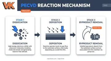
Chemical byproducts desorb from the substrate surface and are pumped out of the chamber, completing the cycle.
Process Parameters and Film Control
The two-stage mechanism only delivers consistent results when process parameters are tightly controlled. Plasma-Therm's optimization work on low-stress silicon nitride shows how precisely these variables can be dialed in: by adjusting NH₃ flow, N₂/(N₂+He) flow ratios, and RF power, engineers tuned film stress from +300 MPa tensile to -300 MPa compressive while targeting refractive index values of 2.0 to 2.05. Thickness non-uniformity was held below ±2.5%.
Key controllable parameters include:
- RF power — controls plasma density and ion bombardment energy
- Gas flow rates and ratios — determine film stoichiometry and composition
- Operating pressure — standard PECVD typically runs at 1–2 Torr (Plasma-Therm); HDPCVD operates at significantly lower pressures
- Substrate temperature — affects film density and hydrogen content
Key Advantages of PECVD Over Conventional CVD
Lower Deposition Temperature
Plasma supplies the activation energy that heat would otherwise provide, so the substrate stays cool while reactions proceed efficiently — making low-temperature deposition the defining advantage of PECVD over thermal CVD. This matters for:
- Polymers and organic substrates that degrade above 200°C
- Pre-deposited metal interconnect layers in integrated circuits
- Bonded wafer assemblies where adhesives have thermal budgets around 200°C
- Mixed-material assemblies with different thermal expansion coefficients
That temperature sensitivity is precisely what distinguishes PECVD substrates from those used in high-temperature diffusion coatings. Industrial thermal diffusion processes — such as the boronizing and aluminizing services VaporKote provides for wear-resistant industrial components — operate at 800–1000°C to form intermetallic compounds in robust steel and alloy substrates. PECVD targets a different substrate population entirely: temperature-sensitive materials that those processes would damage.
Superior Conformity on Complex Surfaces
PECVD is a gas-phase diffusion process — reactive species surround and coat complex geometries, including trenches, via sidewalls, and stepped surfaces. PVD, by contrast, is a line-of-sight process. As the University of Michigan LNF documents, evaporated PVD films have poor sidewall coverage and leave shadowed areas on non-planar surfaces. For high-aspect-ratio features in semiconductor devices, PECVD conformity is essential.
Precise Film Property Control
By adjusting plasma parameters without changing the base chemistry, engineers can tune:
- Electrical conductivity and dielectric constant
- Optical refractive index (PECVD SiNx spans 1.55 to 2.79 depending on process conditions)
- Mechanical hardness and internal stress
- Film density and hydrogen incorporation
Unique Material Capabilities
PECVD can produce materials unavailable through standard thermal CVD, including Diamond-like Carbon (DLC) — deposited using precursor gases such as CH₄, C₂H₂, or C₆H₆. DLC films exhibit high hardness, low friction, and strong wear resistance, making them relevant to tribological applications across mechanical, automotive, and aerospace components.
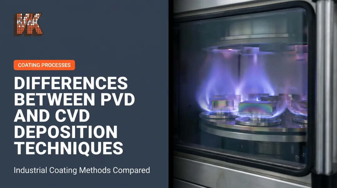
PECVD vs. CVD vs. PVD: Key Differences
Fundamental Process Distinction
CVD and PECVD are both chemical processes: gaseous precursors react to form a solid film on the substrate surface. PVD works differently — solid source material is sputtered or evaporated, then condenses on the substrate. PECVD is a plasma-assisted subset of CVD, not a hybrid of the two technologies.
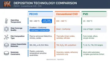
Comparison Table
| Attribute | PECVD | Conventional CVD | PVD |
|---|---|---|---|
| Operating temperature | Room temp to 350°C | 600–800°C | 150–500°C (Oerlikon) |
| Step coverage | Excellent (gas-phase diffusion) | Good to excellent | Poor (line-of-sight) |
| Film composition | Chemically tailored | Chemically tailored | Primarily elemental |
| Unique materials | DLC, SiNx, SiO₂, amorphous Si | Intermetallics, carbides at high temp | Nitrides, pure metals |
| Substrate constraints | Broad — low thermal budget | Limited to high-temp substrates | Moderate — geometry-sensitive |
The table above highlights where each process excels, but the right choice depends on your specific application requirements.
Selecting Between Technologies
Neither PECVD nor PVD is universally superior. The right choice depends on:
- Temperature-sensitive substrates point toward PECVD; robust metals can tolerate PVD or thermal CVD
- Complex three-dimensional features and high-aspect-ratio structures favor PECVD; flat or simple geometries are equally served by PVD
- Chemically complex or compound films suit PECVD; high-purity elemental coatings favor PVD
- Extreme wear and high-temperature service often call for thermal diffusion processes like boronizing or aluminizing, which form metallurgical bonds rather than surface coatings
Common Applications of PECVD
Semiconductors and Microelectronics
PECVD is a foundational process in semiconductor fabrication. Primary uses include:
- Dielectric layers — silicon dioxide (SiO₂) and silicon nitride (Si₃N₄) insulate conductive layers in integrated circuits
- Passivation layers — protect finished devices from moisture, ionic contamination, and mechanical damage
- Advanced packaging — via-last TSV liners, inter-die gap-fill, hybrid bonding, and via-reveal passivation at thermal budgets as low as 100–110°C
Solar and Optical Coatings
Plasma-deposited hydrogenated silicon nitride (a-SiNx:H) is the leading antireflection coating for silicon wafer solar cells (as documented in peer-reviewed photovoltaics research). PECVD SiNx films at n = 2.0 and 70 nm thickness achieve weighted average reflectance below 2.5% on textured silicon surfaces — enabling higher photon capture and improved cell efficiency.
The same refractive index tunability (1.55 to 2.79 for SiNx alone) makes PECVD valuable for precision optical coatings on sunglasses, optical glass, and photometric instruments.
Biomedical and Tribological Applications
PECVD's ability to produce ultra-pure, chemically inert films at low temperatures opens two biomedical pathways worth noting:
- PE-CVD SiOx films on implant ceramics demonstrate hydrolytic stability suited to long-term implant environments (biocompatibility must be validated per ISO 10993-1 for each specific device)
- PECVD-deposited DLC films on M2 steel show wear rates as low as 0.001901 mm³/N·m with a TaN interlayer (2025 study), demonstrating strong durability against 100Cr6 steel under both dry and lubricated conditions
Types of PECVD Reactors and Plasma Sources
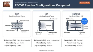
Capacitively Coupled Plasma (CCP) — Direct PECVD
The most common configuration: plasma is generated between two parallel plate electrodes inside the chamber, with the substrate exposed directly to the plasma. Advantages include lower equipment cost and simpler operation. The tradeoff is potential ion bombardment damage to the substrate and electrode material incorporation in the film.
Inductively Coupled Plasma (ICP) — Remote PECVD
An inductive coil generates plasma externally, keeping the electrodes outside the deposition zone. Oxford Instruments describes ICP CVD modules as producing high-quality films at high plasma density and low process pressures. Benefits include cleaner films with less contamination — better suited for damage-sensitive substrates where ion bombardment would degrade performance.
High Density Plasma PECVD (HDPCVD)
HDPCVD combines CCP (for substrate bias) with ICP (as the plasma source), achieving plasma densities of 10¹¹ to 10¹² ions/cm³ — roughly 1,000× higher than the 10⁸ to 10⁹ ions/cm³ typical of standard parallel-plate PECVD. According to Plasma-Therm, it also operates at lower process pressures than standard PECVD.
That combination unlocks a key capability: Lam Research notes that HDP-CVD balances simultaneous deposition and sputtering to prevent bread-loafing and achieve void-free gap-fill in high-aspect-ratio spaces, which is critical in advanced semiconductor manufacturing.
Frequently Asked Questions
CVD vs. PVD: Which is better for thin-film deposition?
Neither is universally better. CVD (including PECVD) provides better step coverage on complex geometries and enables chemically tailored films across a wide temperature range. PVD delivers high-purity elemental or nitride coatings with simpler process chemistry. The right choice depends on substrate thermal tolerance, required film chemistry, and component geometry.
What are the advantages and disadvantages of PECVD?
PECVD offers meaningful process advantages alongside real tradeoffs worth understanding before specifying it.
Advantages:
- Low deposition temperature — compatible with temperature-sensitive substrates
- Excellent conformity on complex geometries
- Tunable film properties and broad material capability, including DLC
Disadvantages:
- Higher equipment cost than conventional CVD
- Hydrogen incorporation in certain films (particularly SiNx:H)
- Requires precise process control and vacuum operating conditions
How is ALD different from CVD?
Atomic Layer Deposition (ALD) is a self-limiting, sequential process that deposits material one atomic layer per cycle (typically 0.1–3.0 Å/cycle), enabling extreme thickness precision and pinhole-free films. CVD and PECVD deposit films continuously through simultaneous gas-phase reactions — much faster for thicker coatings, but without ALD's atomic-level thickness control.
What materials can be deposited using PECVD?
PECVD can deposit silicon dioxide (SiO₂), silicon nitride (Si₃N₄), amorphous silicon (a-Si:H), silicon oxynitride (SiON), silicon carbide (SiC), and Diamond-like Carbon (DLC). Precursor gas selection determines the film — for example, SiH₄ + N₂O produces SiO₂, while hydrocarbon gases such as CH₄ or C₂H₂ yield DLC.
What is the typical operating temperature range for PECVD?
Standard PECVD operates between roughly 200–400°C, with advanced packaging applications achieving production-qualified films as low as 100–110°C. Conventional thermal CVD, by comparison, typically requires 600–800°C — a range many substrates cannot tolerate.